FPGA programming plays a critical role in digital design, particularly when it comes to implementing precise timing and delays. Whether you’re building data pipelines, signal processors, or high-speed communication systems, understanding how to achieve delay in an FPGA environment is fundamental. This blog covers key methods for implementing delay in FPGA programming—from simple to highly accurate solutions—and provides students with a practical foundation.
What is FPGA Programming?
FPGA programming refers to the process of configuring a Field-Programmable Gate Array (FPGA)—a type of digital integrated circuit—so it performs a specific hardware function. Unlike traditional microcontrollers that run software, FPGAs are programmed to behave like actual hardware circuits.
Key Concepts:
-
Reconfigurable Hardware: FPGAs can be reprogrammed after manufacturing.
-
Parallel Processing: Multiple operations can run simultaneously.
-
Hardware-Level Control: Ideal for timing-critical and high-speed applications.
FPGA programming involves writing hardware description code using specific languages, compiling it, and uploading the bitstream to the FPGA chip.
Types of FPGA Programming Languages
There are several languages used for FPGA programming, mainly hardware description languages (HDLs):
1. Verilog
-
C-like syntax
-
Widely used in industry
-
Good for designing logic circuits and modules
2. VHDL (VHSIC Hardware Description Language)
-
Strongly typed and verbose
-
Popular in Europe and aerospace/defense sectors
-
Good for complex designs with strict reliability
3. SystemVerilog
-
Extension of Verilog with high-level features
-
Useful for testbenches and simulation
4. OpenCL (for HLS – High-Level Synthesis)
-
Allows writing FPGA code in a software-style approach
-
Used in data-center and AI workloads
Why Delay Matters in FPGA Programming
Delays are crucial in FPGA programming for a wide range of reasons:
-
Synchronizing signals
-
Managing data buffering
-
Ensuring setup/hold timing constraints
-
Aligning input/output data in high-speed interfaces
Without proper delay implementation, even a well-coded design can result in unstable or incorrect behavior.
FPGA Delay Implementation
Implementing delay in FPGA design is a fundamental skill in digital circuit design—but it’s filled with potential pitfalls and complexities. Based on years of practical experience, this guide introduces six mainstream techniques for implementing delays in FPGAs. These range from picoseconds to seconds and include best practices for avoiding common mistakes, along with recommendations for selecting the right method for your application.
1. Basic Method: Register Staging
Principle:
Cascading multiple D flip-flops (DFFs), each stage introducing one clock cycle of delay.
Code Example (Verilog):

Use Case:
Fixed short delays (e.g., clock domain crossing, pipeline insertion).
Pros:
-
Low resource usage
-
Good timing control
Cons:
-
Delay resolution limited by clock frequency
-
Cannot achieve sub-cycle delay
Tip:
In Vivado, apply “set_max_delay” constraints to prevent optimization across flip-flop stages.
2. Resource Swap: Shift Register
Principle:
Use LUTs configured as shift registers (e.g., Xilinx SRL16E) for delays of 1–32 clock cycles.
Code Example (Verilog):
Use Case:
Medium delays (e.g., video line buffering, data alignment).
Pros:
-
Saves flip-flop resources
-
Supports dynamic delay configuration
Cons:
-
Consumes LUTs
-
Cascading required for >32 cycles
-
Possible timing issues
Example:
In an image processing project, SRL16E was used to achieve a 24-cycle delay, saving 30% of flip-flop resources.
3. Flexible Control: Counter-Based Delay
Principle:
A counter tracks clock cycles and triggers an output at a preset value.
Code Example (Verilog):

Use Case:
Programmable long delays (e.g., LED blinking, FSM timeout).
Pros:
-
Wide delay range (1 cycle to seconds)
-
Parameterizable design
Cons:
-
Delay must be shorter than signal interval to avoid event loss
Optimization Tip:
Combine with PWM techniques and high-frequency clocks (e.g., 50 MHz) to achieve ±20 ns accuracy.
4. FIFO/RAM Buffering
Principle:
Use Block RAM or distributed RAM to cache data and control delay through read/write pointers.
Implementation:
-
Small data volume: Shift RAM IP core
-
Large data streams: Custom FIFO + dual-port RAM
Use Case:
Large data stream delay (e.g., video frame buffering, radar echo simulation).
Example:
A 5G base station used 36Kb BRAM to achieve 1ms baseband delay with 10Gbps throughput.
Notes:
-
Carefully calculate memory depth to avoid overflow
-
Use Gray code in asynchronous FIFOs to safely cross clock domains
5. Hardware Delay Primitives
Principle:
Use built-in delay units (e.g., Xilinx IDELAYE2) and adjust delay using tap settings.
Key Parameters:
-
Approx. 78 ps delay per tap (at 200 MHz reference clock)
-
Max 31 taps = ~2.4 ns delay
Code Example (Verilog):

Use Case:
High-speed SerDes timing alignment, DDR eye diagram optimization.
Pitfall Avoidance:
-
Use the IDELAYCTRL module for calibration
-
Keep reference clock jitter below 50 ps
6. PLL Cascading
Principle:
Cascade multiple PLLs/DLLs to generate phase-shifted clocks for picosecond-level delays.
Examples:
-
Cyclone IV PLL cascade achieving 10 ps step delay
-
Xilinx 7-series MMCM with phase interpolation
Use Case:
High-precision interleaved sampling (e.g., oscilloscope ADC calibration)
Drawbacks:
-
Consumes PLL resources
-
VCO frequency limitations (e.g., Xilinx UltraScale+: 600–1200 MHz)
Delay Solution Selection Guide
|
Delay Requirement |
Recommended Method |
|---|---|
|
Short (<10 ns) |
IDELAYE2 Primitive > Register Staging |
|
Medium (10 ns–1 ms) |
Counter-Based Delay > Shift Register |
|
Long (>1 ms) |
FIFO + External DDR > Large Capacity BRAM |
|
Picosecond Precision |
PLL Phase Interpolation + IDELAYE2 |
Common FPGA Programming Software Tools
To write, simulate, synthesize, and deploy FPGA designs, engineers and students use specialized software suites:
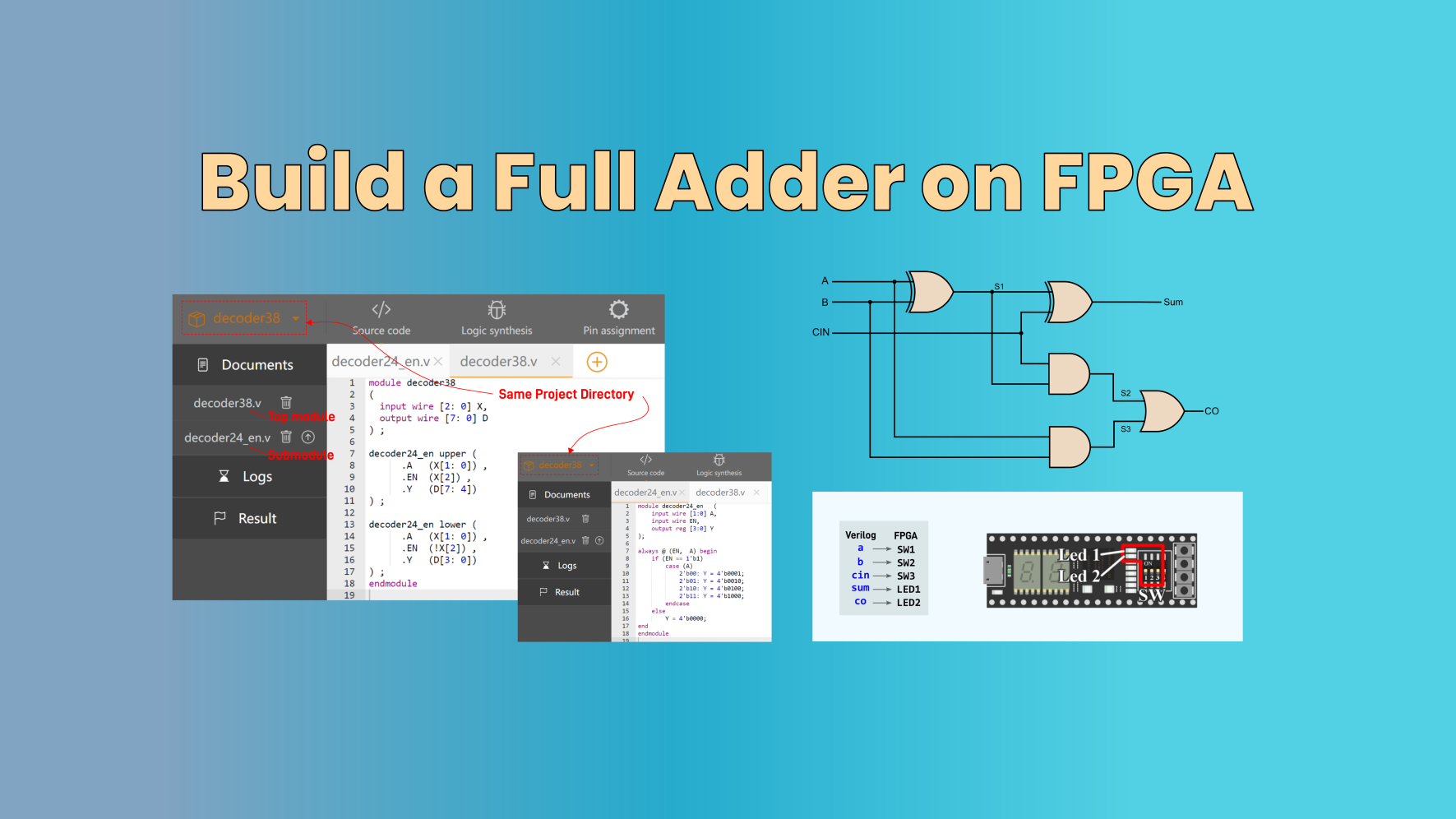
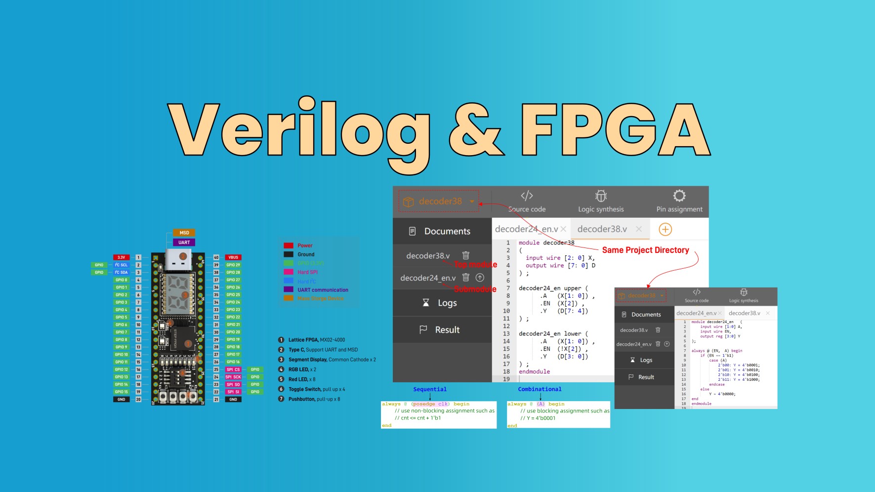
1. EIM Technology StepFPGA Web IDE
-
A beginner-friendly FPGA programming tool built specifically for education
-
Fully web-based—no installation required
-
Supports Verilog programming for the StepFPGA development board
-
Ideal for students learning digital logic and delay techniques
-
Access it directly at EIM StepFPGA IDE or EIM Support
2. Xilinx Vivado
-
Used with Xilinx FPGAs (e.g., Artix, Zynq)
-
Includes simulation, synthesis, implementation, and bitstream generation
3. Intel Quartus Prime
-
For Intel/Altera FPGAs (e.g., Cyclone, MAX)
-
Offers a user-friendly interface and wide tool integration
FAQs: FPGA Programming and Delay Design
Q1: What is the simplest way to implement delay in FPGA programming?
A: Cascading D flip-flops is the simplest and most resource-efficient method for fixed delays.
Q2: Can I create delays smaller than one clock cycle?
A: Yes, by using FPGA primitives like IDELAYE2 and PLL phase shifts, you can achieve sub-cycle delays.
Q3: Is counter-based delay suitable for high-speed designs?
A: It depends on your system clock. High-frequency clocks allow finer resolution, but for ultra-fast designs, hardware primitives are preferred.
Q4: What’s the best FPGA board for learning delay techniques?
A: Xilinx Basys 3 is highly recommended for students due to its beginner-friendly environment and good documentation.