Nodal voltage analysis and mesh analysis are two well-known techniques among them. In nodal voltage analysis, the first step involves selecting a node as a reference node. This node is usually assumed to have an absolute zero potential and is commonly referred to as the "ground" node.
If you're not paying attention to the voltage relationships between the circuit and other objects, you generally won't notice any harm in this assumption. Choosing a shared node among multiple subcircuits as the ground node is often an excellent choice for simplifying circuit analysis mathematically.
When studying electronic circuit courses, we often overlook many circuit analysis techniques, such as superposition, Thevenin Equivalent, Norton Equivalent, mesh analysis, etc. This article mainly focuses on one such technique, nodal voltage analysis (see Figure 1).
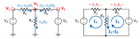
Figure 1: Node voltage analysis typically simplifies the analysis of electronic circuits. On the left is an example of node voltage analysis, while on the right is an example of mesh analysis for the same circuit.
After years of in-depth study during my student days and engineering career, one might forget some basic concepts in electronic circuit theory, and this is precisely when serious misconceptions can seep into our thinking.
Common Misconceptions:
The ground node is often mistaken as the physical "graveyard" where all charges terminate. This is certainly not true; the ground node is simply a node of our personal choice. Besides being the common node for many subcircuits, it has no special significance. Being a common node does not confer any special physical properties. The only charges stored at the ground node are those on the negative plate of a capacitor connected to ground. All other charges flow through the circuit and never come to a halt (see Figure 2). Remember, all currents flow in a loop, and charges return to their source.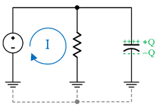
Figure 2: Current charges circulate in a loop, and the only stored charge (-Q) at the ground node is the charge on the capacitor connected to ground.
The ground node as a safe haven to avoid noise? This is not entirely correct either; most different noise currents will flow through the ground node (see Figure 3). However, for well-designed ground traces, the impedance of the conductive trace can be negligible, resulting in almost zero potential difference across the traces for noise.
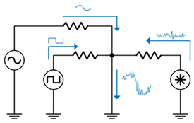
Figure 3: Different signal currents and different noise currents flow through the ground node. The low impedance of the ground trace is the only guarantee to ensure that the potential difference between any two physical points in the conductive trace can be neglected, at least in DC circuit analysis.
If the domains of two ground pads affect each other, could isolating them protect the quiet domain from the influence of the noise domain? This might be one of the most serious mistakes made by RF engineers without realizing it. In various cases, isolating ground pads may lead to severe noise coupling from the noise domain output to the quiet domain input. This may seem counterintuitive, but it becomes clearer when you draw the complete circuit using wires up to the circuit board (PCB) layers, as shown in Figure 4. Similar effects can also occur when all metal-oxide-semiconductor (MOS) blocks are connected to dedicated ground pads.
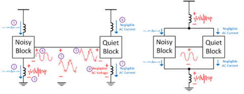
Figure 4: When isolating the ground pad on the left side of the diagram, many noises occur when signals are transmitted from one domain to another. The analysis steps are marked with purple circles. On the other hand, as shown on the right side, combining domains allows signals to be transmitted safely. However, if the Power Supply Rejection Ratio (PSRR) is poor, the Quiet Block may be affected.
In the design of digital circuits considering power consumption, floating outputs are not only related to breaking the ground path but also to breaking the power supply path (see Figure 5). Physical design preferences typically lean towards switching the ground path. This is because under the same ON resistance, NMOS devices, which have a smaller area than PMOS devices, will be used.
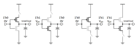
Figure 5: When the power supply or ground is turned off, it inevitably may lead to uncertain output voltages. This uncertain output voltage depends on the last operating output state stored on the load capacitor, the ratio of OFF resistance between the power supply and ground, and the leakage currents at different points.
Ground and power traces seem unrelated to timing convergence. Timing convergence relates to different unit delays and different signal edges. When the ground trace has relatively high impedance, significant IR drop occurs between the power and ground traces, reducing the effective power supply voltage and thus increasing the delay of CMOS units. Additionally, even if the average IR drop on the power trace is negligible, switch noise currents can generate significant transient noise voltages on the ground trace.
Therefore, as shown in Figure 6, the signal edge reaching the gate of the farthest signal source can be effectively "shifted" in time. The time shift depends on the magnitude and polarity of the transient noise. This effect becomes more pronounced for signals with high rise/fall times.
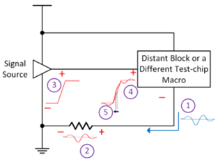
Figure 6: According to the analysis steps indicated by the purple circles, transient power/ground current curves will generate similar voltage curves at the ground terminal, affecting the effective arrival time of signal edges. Substantially increasing local decoupling capacitors to absorb alternating current (AC) current curves and reducing the impedance of power/ground traces can alleviate this issue.
Whether or not to isolate ground pads?
This is a tricky question that requires detailed explanation. The previous content may give the impression that isolating ground pads is a poor design practice, but in many chips, this may be a common approach. Typically, designing a single unified ground with low resistance and low inductance is far superior to designing multiple ground traces. Multiple ground traces can cause some troubles, such as complex return current paths between multiple domains and magnetic coupling due to large-area loops carrying high-frequency currents.
However, in some cases, isolating ground pads is unavoidable. For example, suppose you have a crystal oscillator and a digital block with noise sharing a ground pad, as shown in Figure 7. The digital block draws noise current from the power supply and returns it through the ground trace and solder joints. Therefore, there will be significant voltage faults on the ground line. Since this solder joint shares ground with the crystal oscillator, the noise voltage fault actively loads the crystal's internal node with the pure sine voltage of the crystal.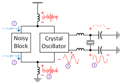
Figure 7: According to the analysis steps indicated by the purple circles, noise blocks indirectly generate noise voltage at the ends of the ground solder joints. Since the crystal essentially acts as a bandpass filter with good cutoff characteristics, there is a pure sinusoidal voltage present on each terminal during oscillation. However, internal nodes of this crystal oscillator will detect the superposition of pure voltage and noise voltage on the entire ground line.
In situations requiring isolation of ground pads, please perform the following actions:
- Place multiple decoupling capacitors around the noise blocks as much as possible (see Figure 8). This will reduce the transmission of noise power supply current externally to the chip, thereby minimizing the noise voltage generated by the conducting track of this block and its output.
- Minimize electrical interaction between the noise block and other blocks, or simply reduce the current passing between them. To achieve this, use drivers with relatively high output impedance in the noise domain, and drivers with high input impedance buffers in the quiet domain.
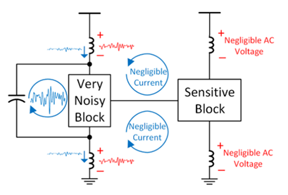
Figure 8: The decoupling capacitors at the noise block terminals absorb most of the AC current flowing through the power supply and ground. Minimizing the transmission current from the noise domain to sensitive blocks ensures minimal transmission of noise.
The ground node is just a node defined for circuit analysis; all currents still flow in loops and do not terminate at the ground node.
To predict and address ground-related issues, it's sufficient to draw the complete circuit with all physical connections without necessarily defining ground nodes, allowing different current loops and shared paths to be visualized.
Before deciding to unify or isolate ground pads from different domains, it's essential to understand the expected gains and potential impacts carefully. As shown in Figure 9, this is an exercise where the left side displays a simple NMOS current source with finite drain impedance. So, what is the low-frequency AC impedance of the power supply voltage source?
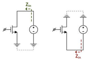
Figure 9: Does the definition of the ground node affect the input impedance value?
The answer is very simple. Keeping the circuit unchanged in physical terms but selecting the NMOS drain as the ground node instead of the NMOS source, as shown on the right side of Figure 9, will the impedance remain unchanged? Don't let the grounding misconception confuse you.